A new Ultra high resolution, Electron Beam Lithography instrument is now available at CMM.
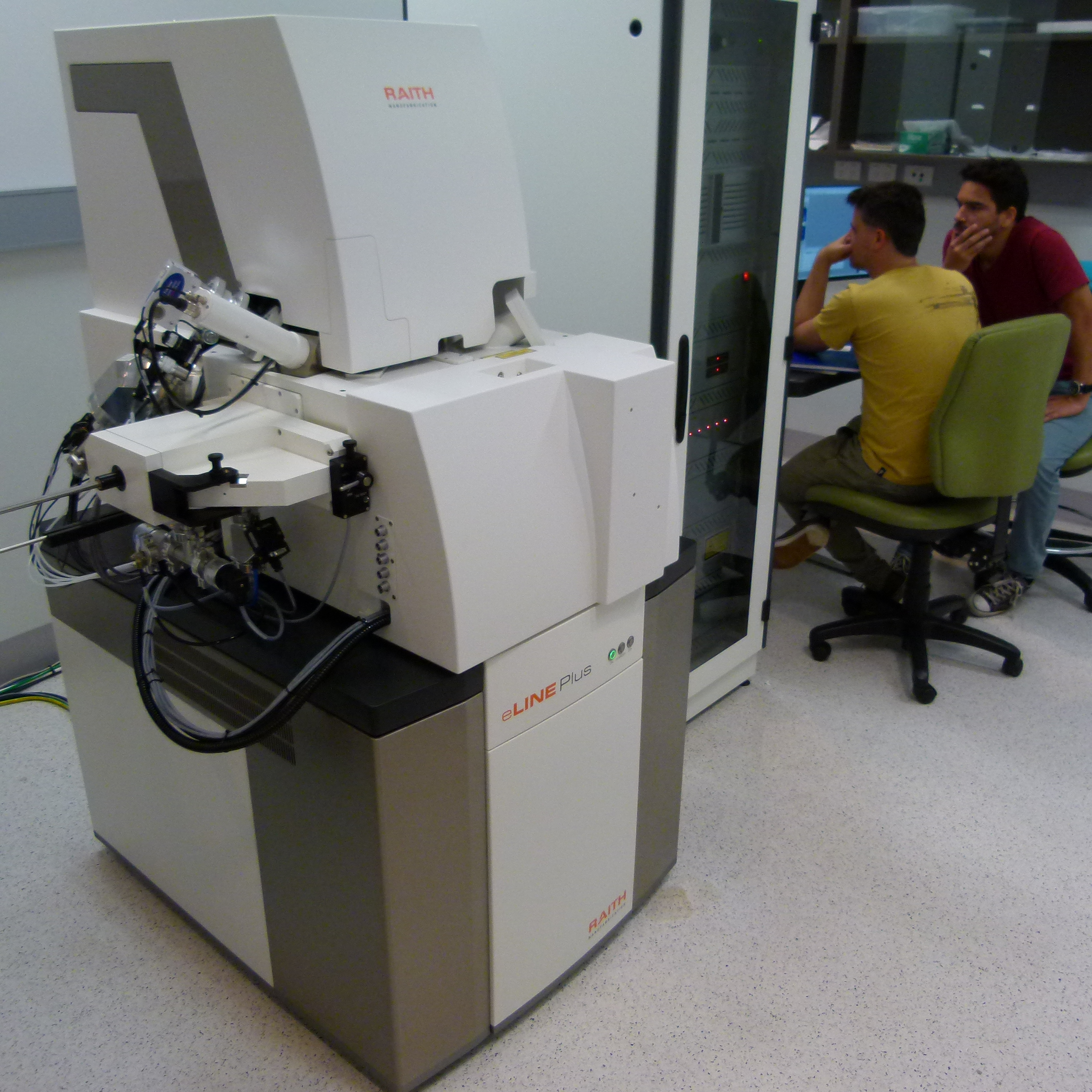
Installed in early June, the RAITH E-Line Plus provides the essential tools required for Nano Fabrication processes and techniques at The University of Queensland.
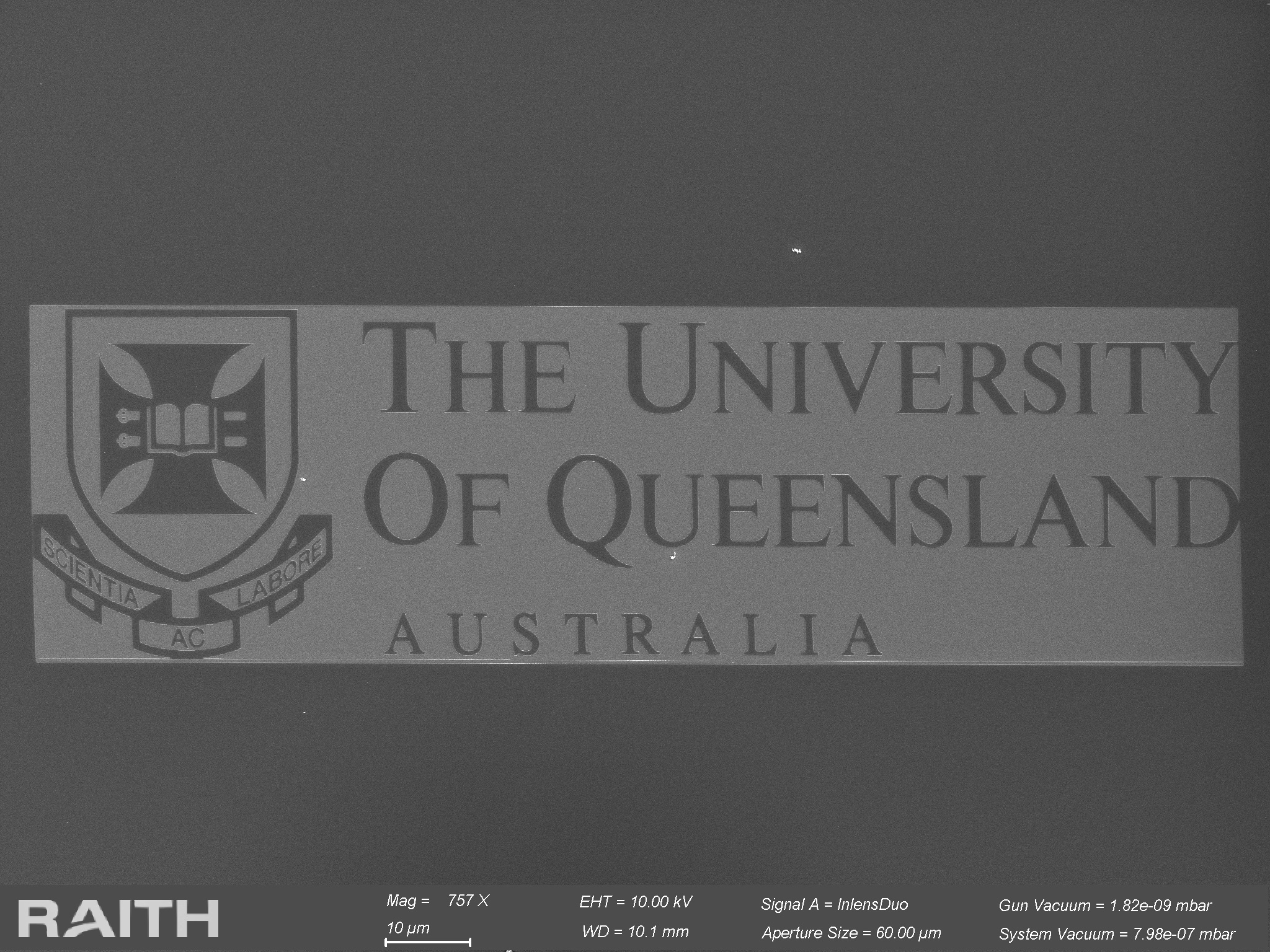
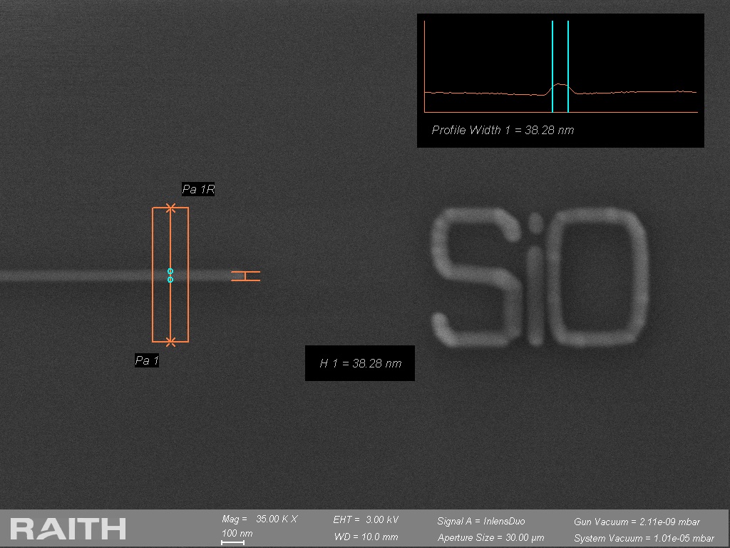
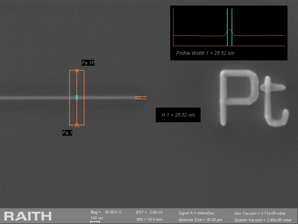
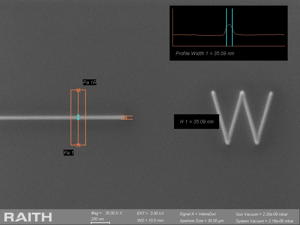
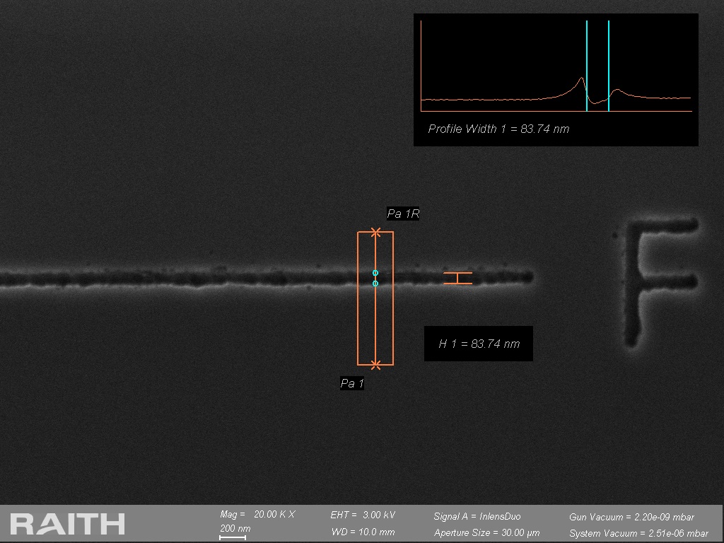
The instrument is based at the CMM, AIBN Laboratory. It caters to a variety of different applications: SEM imaging and analysis; Nano lithography; Nano manipulation and Focused Electron Beam Induced additive fabrication by material deposition (Images 2, 3 and 4) and subtractive fabrication by etching (Image 5).
|
|
|
| Image 2: 38.3nm Line width of insulating material Silicon Monoxide. |
Image 3: 25.5nm Line width of Platinum. |
|
|
|
| Image 4: 35.1nm Line width of Tungsten. | Image 5: 83.7nm Line width etched with Fluorine. |

At the time of installation, tests were run and beam size results showed that at1keV using the 30mm aperture the beam size was 3.4nm. A 1.5nm beam size was achieved at 20keV.
The E-Line Plus is a specialised tool with high resolution capabilities; able to expose features that are less than 10nm in size (Image 6).
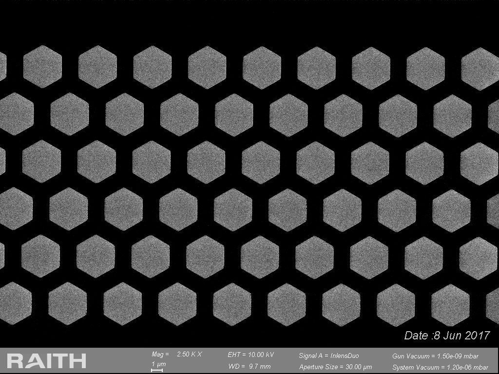
A Honeycomb structure is one of many designs the RAITH E-Line Plus can produce using a technique called Modulated Beam Moving Stage (MBMS). The MBMS patterns are 2 mm long and each pattern consists of three MBMS stripes (Image 7).
(Images 2-7 Courtesy of Dr Keith Moulding, Onsite Qualification Report 3-000-259 University of Queensland, Brisbane. 16th June 2017, Raith GmbH)


